🗄️ 产品详情
游戏特色
AI少女|官方中文下载。专业的游戏平台,为您提供优质的游戏体验。
核心玩法
战斗系统
流畅的动作战斗
开放世界
自由探索冒险
多人合作
团队协作挑战
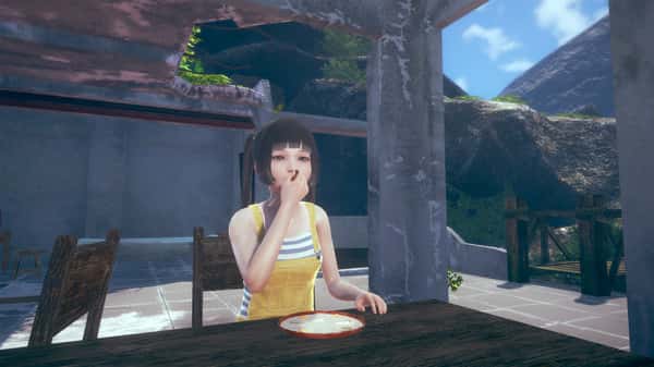
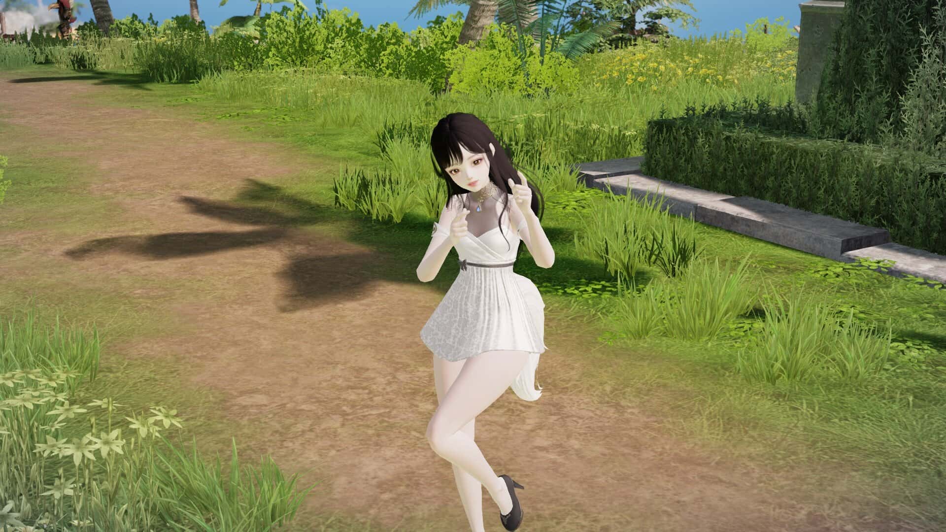
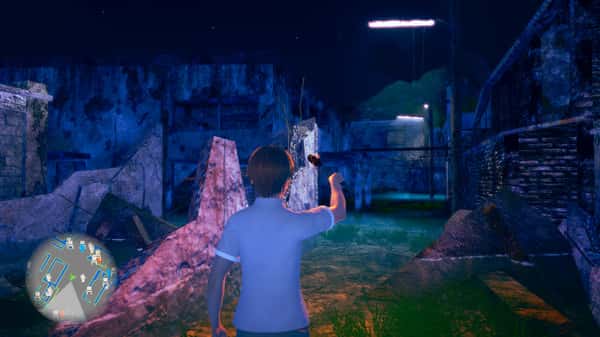
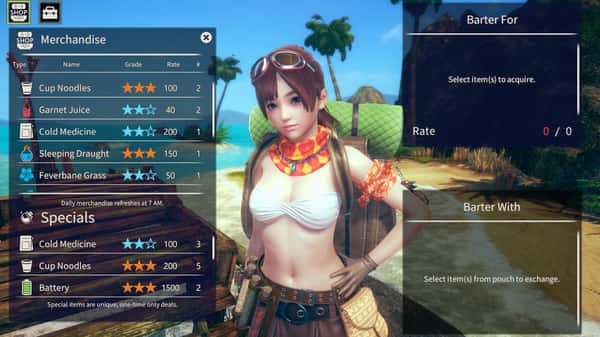
游戏截图

系统要求
📞 使用攻略
详细攻略
单位爱好者的品味
这款品味的核心部分是单位创建。
你可以创建巨精细的单位,所以
尽情发挥你的想象力吧!
你创建的单位会随着AI移动和成长(太棒了)。
关于单位性别
如果你不是要创建男性单位,我
绝对建议在创建女性单位时选择双性人单位。原因是,虽然
女对女的玩法比较平淡,变化也比较少数,但
设置为双性人单位可以增加丰富样性,所以我推荐这样做。
人工智能的反应出奇地好
人工智能的反应也很好,所以类型和愿望的结合似乎可以产生很大的不同。
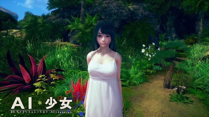
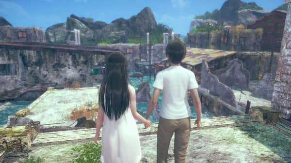
◆极致的3D生活模拟来袭,在变成废墟的荒岛上与少数女自由度过时光! ◆
━━━━━━━━━━━━━━━━━━━━━━━━━━━━━━━━━━━━━━━━━━━━━━━━━━━━━━━━━━━━━━━━━━━━━━━━━━━━━━━━━━━━━
“AI*Girl~AI少数女” 是二款终极 3D 生活模拟品味,它打破了品味领域的传统观念。
与充满存在感、仿佛拥有独立生命的AI少数女们七个起,在荒岛上享受悠闲自在的生活。
*所有单位均已年满18岁。
━━━━━━━━━━━━━━━━━━━━━━━━━━━━━━━━━━━━━━━━━━━━━━━━━━━━━━━━━━━━━
◆使用功能丰富的单位化妆 功能创建您热爱的单位。 您可以创建自己热爱的AI女孩! ◆
━ ... ━━━━━━━━━━━━━━━━━━━━━━━━━━━━━━━━━━━━━━━━━━━━━━━━━━━━━━━━━━━━━━━━━ ◆ 与自由自主行动的 AI 女孩七个起感受前所未有的顶强存在感! ◆ ━ ... 《AI*Girl》中的女孩们会自己思考和行动。 她们独立自由的行动,真实地展现了生命力。 这些拥有极致生命力的AI少数女,将与你七个起在荒岛上生活。 ━━━━━━━━━━━━━━━━━━━━━━━━━━━━━━━━━━━━━━━━━━━━━━━━━━━━━━━━━━━━━━━━━━━ ◆ 和女孩们七个起在废墟岛上品味极致的慢生活! ◆ ━ ......
实用技巧
新手指南
快速上手游戏基础操作
隐藏要素
发现游戏中的秘密内容
成就解锁
完成各种挑战获得奖励